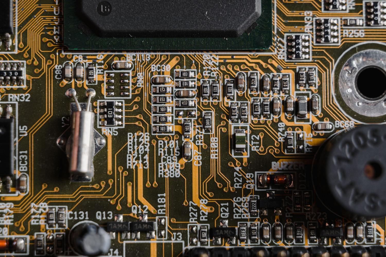
When we delve into the world of printed circuit board design, especially with components operating at maximum power or speed, heat becomes our worst enemy. If not managed properly, the PCB's thermal demands can cause your device to go from a technological marvel to a simple paperweight in the blink of an eye, severely impacting the board's functionality and lifespan.
To avoid these problems, it's essential to have a workflow where design and verification go hand in hand. Using tools that allow you to identify hot spots through simulations before sending the board to manufacturing is the difference between a reliable product and one that fails within a few months. This is where elements like thermal pads, thermal paste, and meticulous copper planning come into play.
The role of unified software in heat management
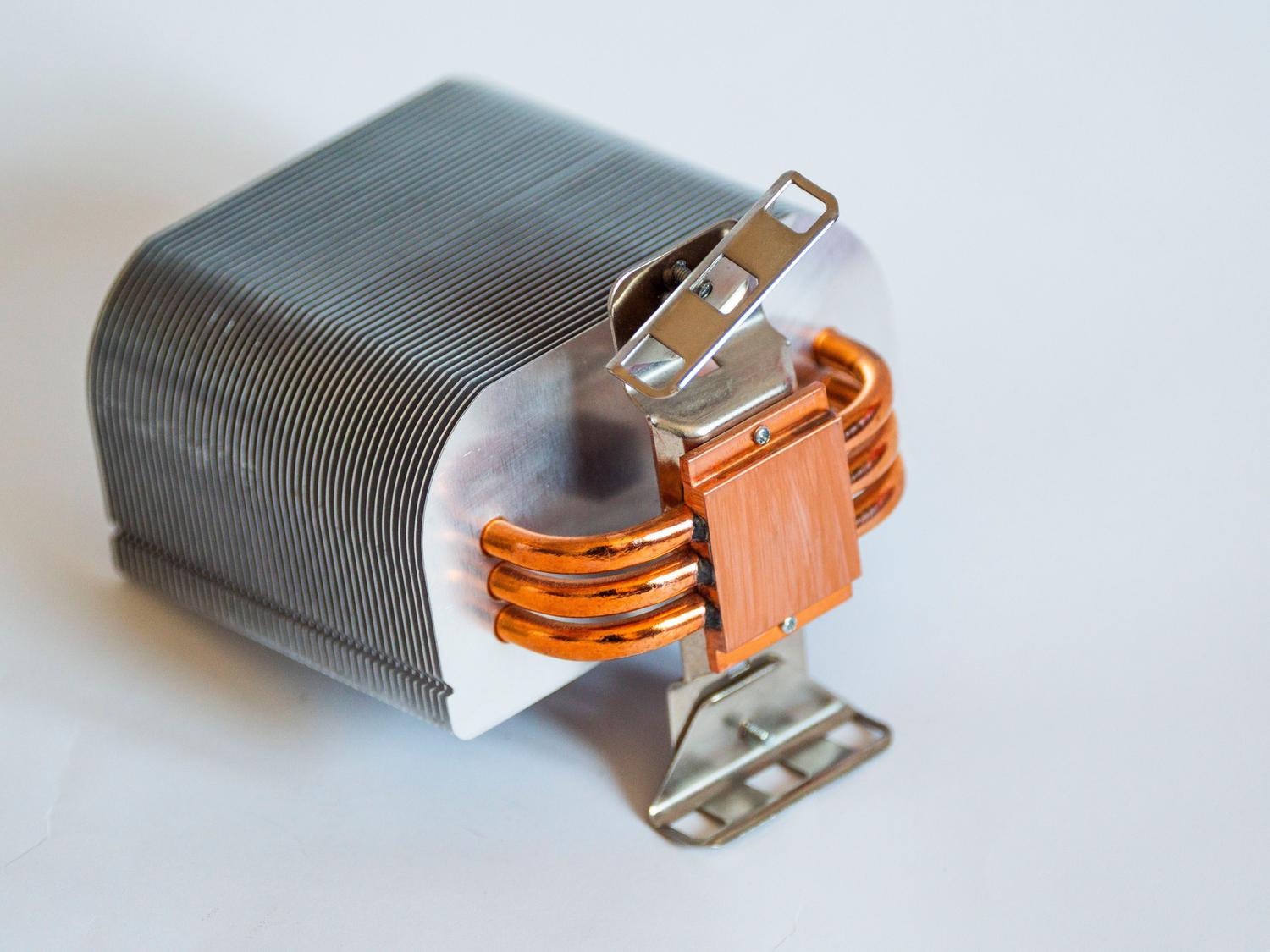
When designing hardware, you have to juggle a thousand things at once: from routing to component selection. Truly useful design software doesn't just draw schematics; it should offer a unified design environment . This means having PCB simulation and creation within the same interface, avoiding the hassle of exporting data between different programs, which often leads to formatting errors and an incredible waste of time.
Thanks to power distribution network (PDN) analyzers, we can visualize where IR losses occur , which are essentially the traces left by hot spots. By detecting these critical areas, the designer can confidently decide where to place a thermal pad or heatsink , optimizing thermal conductivity without cluttering the board with unnecessary components that only get in the way.
Mastering QFN packages and their dissipation
Today, it's very common to use QFN (Quad Flat No-lead) components in RF amplifiers and transceivers due to their compact size. These components have a vital feature: an exposed thermal pad on the underside. This metal square isn't just for show; it conducts heat away from the device and transfers it to the PCB, which acts as the primary heatsink.
Heat in a QFN doesn't travel along a single path; instead, it's distributed in several ways: a small portion radiates into the air, another portion dissipates to the nearby copper in the top layer, and a considerable portion drains down through thermal channels to the inner layers or bottom plane. For this to work, perfect contact between the component and the board is crucial.
The art of soldering the thermal pad without mistakes
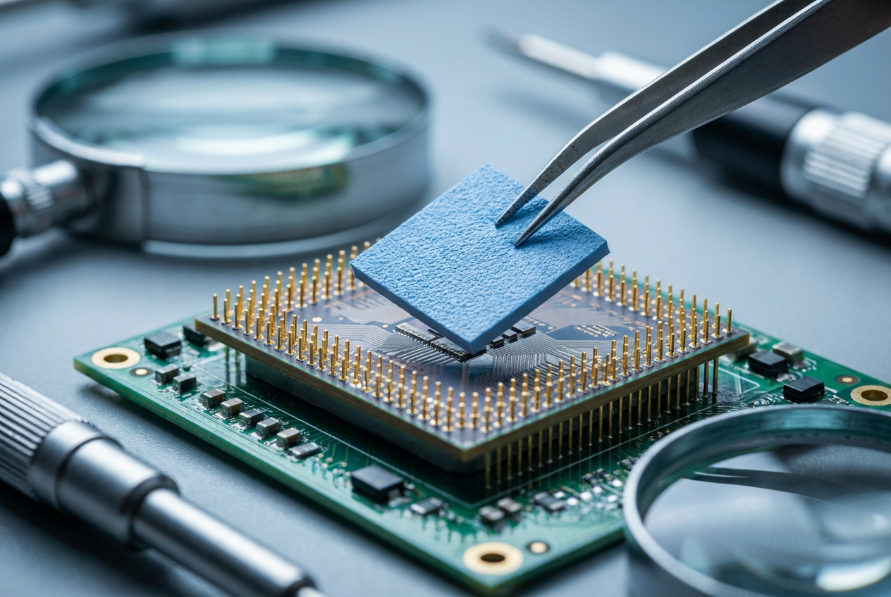
This is where many people go wrong. If you apply too much solder to the center pad of the QFN, the component can "float" on the paste , causing the peripheral pins to lose contact and rendering the board unusable. To avoid this, it's best to use a stencil with a segmented pattern instead of a single, large opening.
There are two main ways to segment the soldering area: using a solder mask or by physically dividing the copper. In either case, it is recommended that the total soldering area represent between 50% and 80% of the total pad area. This not only prevents the component from tilting but also allows the gases generated during the soldering process to escape through the open channels, preventing bubbles that would ruin heat transfer.
Optimization of copper lines and plans
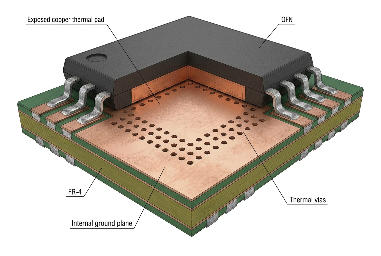
To efficiently transfer heat to the heat sink, solid vias (without thermal relief) must be placed beneath the heat sink. These vias should have an optimized diameter, typically between 0,25 and 0,3 mm, to prevent solder from flowing to the other side of the board. To control this flow, either "Tenting" (covering the vias with masking tape) or "Via Encroaching" can be used , which leaves a small opening at the base to anchor the solder.
Furthermore, simply directing heat to the underside of the board isn't enough; you also need to consider how the heat spreads. It's crucial to avoid running traces parallel to and close to the via array, as these act as thermal barriers . If you absolutely must run a trace there, it's best to do so perpendicular to the center of the device to avoid obstructing heat flow. Extending a wide ground plane around the component on the top layer is also recommended to aid overall heat dissipation.
Real-world alternatives: Pastes, Putty and Pads
When it comes to maintaining devices like laptops, the choice of thermal interface material is critical. Many common commercial thermal pastes tend to degrade quickly in high-temperature environments, a phenomenon known as "pump-out ," where the paste is expelled from the chip by heat cycles. In these cases, solutions like PTM7950 (a phase-change material) are often much more effective than traditional thermal pastes.
For secondary components like VRAM, thermal putty or thermal pads are commonly used. Putty is more versatile because it can be applied at different heights, while pads require precise thickness measurements . If a pad is too thin, it won't make contact; if it's too thick, it can press against the chip, causing other components to detach or resulting in poor contact with the main heatsink. Therefore, choosing the right material based on pressure and height is key to preventing the system from overheating again after just a few months.
The key to successful electronic design lies in the combination of powerful simulation software and precise technical execution in the hardware, taking care of everything from the segmentation of the soldering in the QFN to the correct choice of thermal interface materials to avoid premature component failure.
Table of Contents